
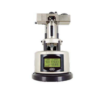
Brand:Bruker
Model:MultiMode8
Industry-Standard AFM for Highest Resolution ImagingDelivering unmatched application flexibility and publication record
· Providing highest resolution imaging and quantitative material property mapping
· Delivering legendary MultiMode versatility
· World's most published AFM
· Powered by PeakForce Tapping
· Though best known for its performance leading resolution, today’s MultiMode® 8 leverages Bruker’s exclusive PeakForce Tapping? technology to provide new information, faster results, and greatly improved ease of use. Bruker’s exclusive ScanAsyst® mode makes imaging easier, faster, and more consistent. One way it does this is by directly controlling the tip-sample interaction force and automatically optimizing imaging parameters. With the new addition of ScanAsyst-HR, MultiMode® 8 scans up to 6X faster for even greater productivity..
· New quantitative material property mapping is made possible using PeakForce QNM®, which analyzes each tip-sample interaction to extract nanomechanical properties including modulus, adhesion, deformation, and dissipation. This can be combined with the new PeakForce TUNA? mode to perform conductivity mapping on even the most delicate samples. With these features and many others, the MultiMode 8 has the versatility to help you excel in virtually any field of research.
Material and Polymer Science
With increasing efforts to rationally design heterogeneous composite materials and a vast library of polymer chemistries and nanoscale building blocks to choose from, characterization methods are needed that map properties at highest spatial resolution. Microphase separations and distribution of additives and fillers affect critical bulk properties in applications from structural materials to organic photovoltaics. To address these characterization needs, the Innova and Dimension Edge provide a full suite of nanomechanical and –electrical modes ranging from phase imaging and force spectroscopy to piezo-response force microscopy, conductive AFM, and Kelvin probe force microscopy, combined with design for highest spatial resolution, achieving atomic resolution with ease.
Electrochemistry
Electrochemical AFM (ECAFM) enables in situ mapping of surface changes while the sample is immersed in the electrolyte and under electrochemical control. Aside from fundamental electrochemistry studies, corrosion and Li battery development stand out as applications of ECAFM. Wide chemical compatibility with aqueous solutions as well as carbonate solvents in the case of Li batteries is key, necessitating use of Teflon/Kel-F as cell material, sufficiently deep and sealable cup-shaped cells, and retention of imaging performance in liquid. Bruker’s new 2nd generation Dimension Icon and Edge electrochemistry cells have been designed specifically to address these issues and provide turnkey solutions for Li battery research.
NanoElectrical Measurement
AFM based nanoscale electrical characterization is well established for semiconductor R&D and FA where scanning capacitance can provide maps of active carrier density and conductive AFM can probe device connectivity and gate oxide breakdown characteristics. Nanoscale electrical properties also play a key role in research areas ranging from graphene to conductive polymers where the most prominent AFM electrical modes are conductive AFM, Kelvin probe force microscopy (KPFM), and electric force microscopy (EFM). Bruker’s Innova and Dimension Edge offer a full suite of electrical modes, leveraging Bruker’s patented LiftMode to enable electric field gradient mapping with EFM, more sensitive KPFM workfunction mapping, and artifact free conductivity mapping with Dark-Lift conductive AFM.
Patterned Sapphire Substrate
Patterned Sapphire Substrate (PSS) is a technique used for LED manufacturers to improve light output and overall device efficiency. A PSS is typically a sapphire wafer into which a periodic pattern has been etched. The patterns' shape vary but are conical, hemispherical, pyramidal or other similar structure. These structures are used to change the angle of outgoing photons reducing total internal reflection and thus increasing efficiency. The Edge-PSS AFM provides the needed metrology to control the PSS fabrication process including feature height, width, and angle measurements while also providing a full 3-D profile. The Edge-PSS is poised to meet the needs of PSS suppliers and LED manufactures as dimensions shrink to gain product efficiency.
Designed for Performance
The legendary performance and reliability of the MultiMode platform is the result of both its superior mechanical design and the industry’s lowest noise control electronics. The secret to its continued presence at the leading edge of AFM research is its ability to incorporate all the latest technology advances.
Faster and More Productive
· The NEW high-speed ScanAsyst-HR is now available, enabling fast scanning on the MultiMode 8 AFM system
· 20X faster survey scan rates and up to 6X faster scans with no loss of resolution
Versatility to Satisfy More Applications
· The MultiMode 8 AFM is equally well suited for imaging in both air and fluid
· Heating to 250°C, cooling to -35°C with temperature control accessories
· A large variety of standard operating modes and many unique capabilities enable the MultiMode 8 AFM system to characterize everything from mechanical to electrical properties
Exclusive & Powerful Quantitative Imaging Modes
· PeakForce QNM enables direct mapping of nanomechanical properties, including elastic modulus, adhesion and dissipation, at high resolution and normal scan rates
· PeakForce TUNA enables quantitative conductivity mapping on delicate samples that can't be imaged with conventional conductive AFM
Click to learn more product information.
Contact our application team immediately: 021-37018108, info@boyuesh.com
Tel:86-021-37018108
Fax:86-021-57656381
Email:info@boyuesh.com
Address:Room 301, 28 Songjiang Hi-tech park, 518 Xinzhuan Road, Songjiang District, Shanghai